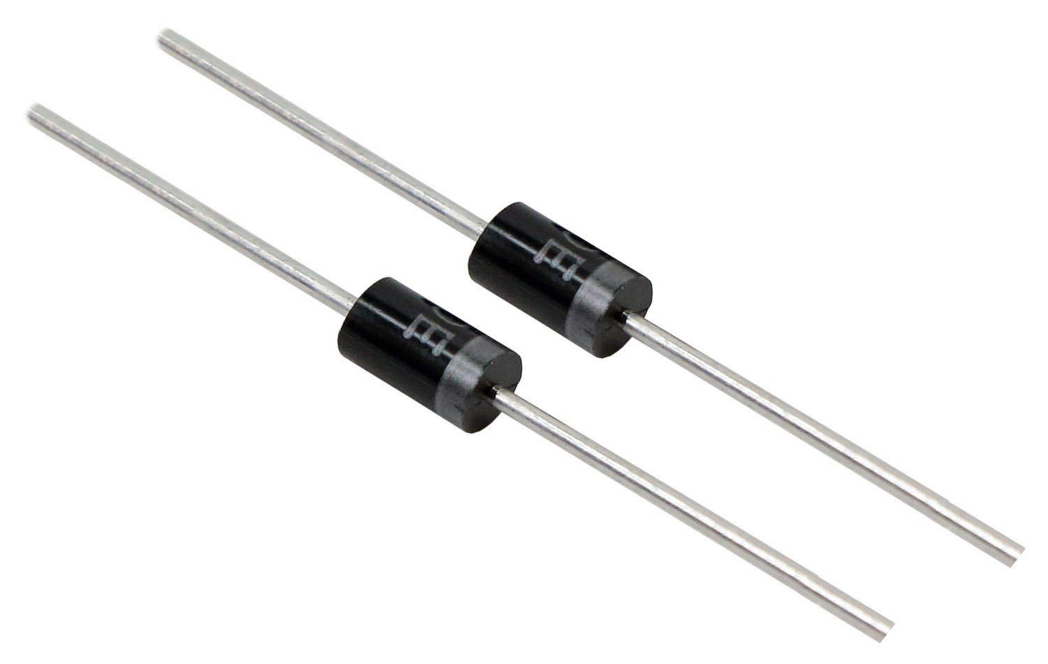
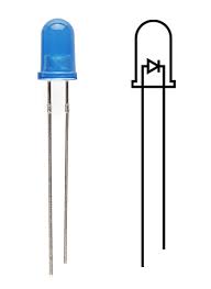
Diodes and LEDs
Brief Description
Everyone uses LEDs in electronics projects but what are they and how do they actually work?
Reccomended Prerequisites:
How It Works
Structure
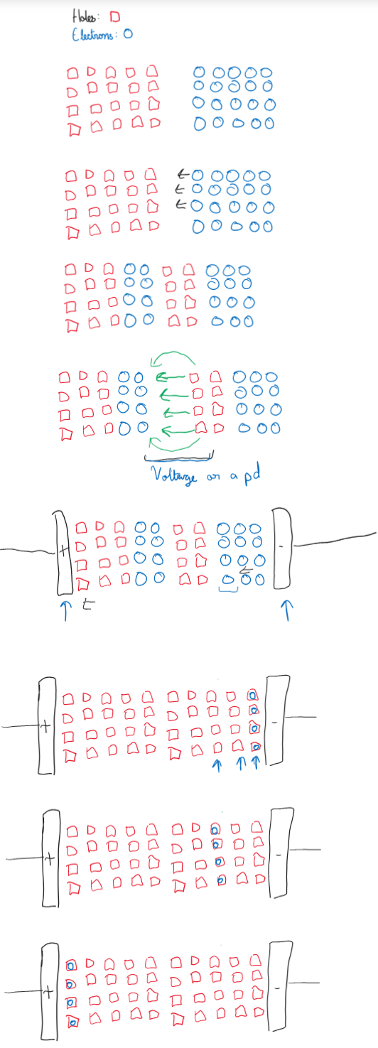
A diode is made from two layers of semiconductor material, one doped with acceptor atoms to create a P-type region (rich in holes) and the other doped with donor atoms to create an N-type region (rich in electrons).
The interface between these two regions is called the P-N junction.
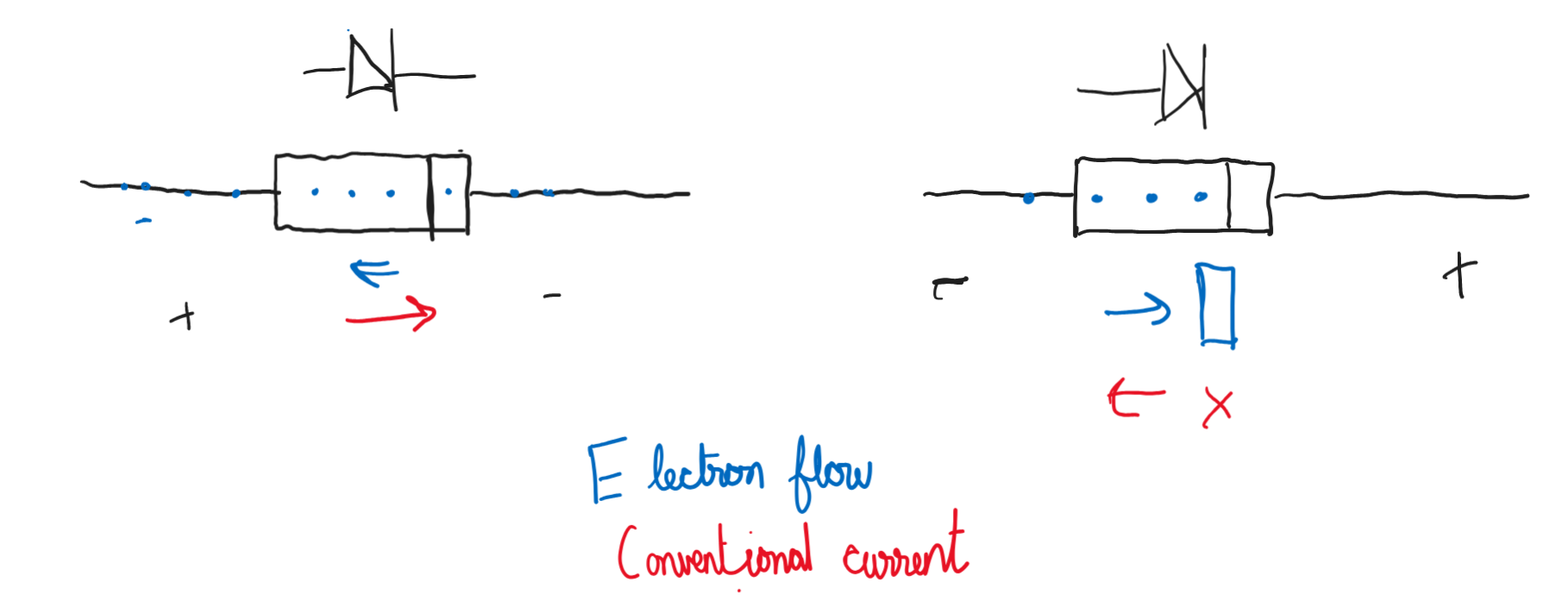
Depletion Region: At the junction, some electrons from the N-type region diffuse into the P-type region and recombine with holes, creating a depletion region where no free charge carriers are present. This region acts as a barrier that prevents current flow under normal conditions.
Biasing the Diode:
Forward Bias:
- When a positive voltage is applied to the anode (P-side) and a negative voltage to the cathode (N-side), the depletion region narrows.
- This reduces the barrier, allowing current to flow across the junction as electrons move from the N-type region to the P-type region and holes move in the opposite direction.
- Result: The diode conducts current.
Reverse Bias:
- When a negative voltage is applied to the anode and a positive voltage to the cathode, the depletion region widens.
- This increases the barrier, preventing current from flowing.
- Result: The diode blocks current.
In forward bias, once the applied voltage exceeds a certain threshold (typically around 0.7V for silicon diodes), the diode conducts, allowing current to flow from the anode to the cathode.
In reverse bias, the diode ideally blocks all current, though a tiny leakage current may flow.
Applications
- Rectification: Diodes are commonly used in rectifiers to convert alternating current (AC) to direct current (DC).
- Signal Demodulation: Diodes can extract information from modulated signals by allowing only certain parts of the signal to pass.
- Protection Circuits: Diodes protect circuits by shunting excess voltage away from sensitive components, as in flyback diodes used in relay coils.
Apparatus Needed
- Diode
- Jumper Wires
- Breadboard
- Arduino
- LED
